LAB EQUIPMENT
ETCHING
LITHOGRAPHY
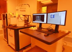
Electron Beam Lithography System: Raith Pioneer

Maskless Lithographic System: Intelligent Micro-Patterning SF-100 XPress

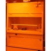
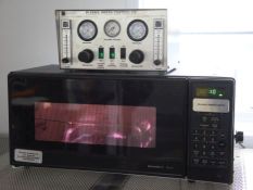
Lithography Sample Preparation: laminar flow hood, spin coater, and baking plates
DEPOSITION
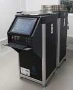
Physical Vapour Deposition (Evaporator): Thermionics 3 kW Linear e-Gun

Chemical Printing System: Sonoplot/GIX Microplotter II Nanoliter Printer
MICROMACHINING

Picosecond Laser Micromachining System: Oxford Lasers A Series
CHARACTERIZATION

Stylus Profilometer: Bruker DektakXT
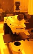
Optical Microscope: Carl Zeiss Axio Imager A1m